������������ɵ�������˾
- Ʒ�ʱ���
- ������һ
- Ʒ����ȫ
Ԫ������Ʒ
COMPONENT PRODUCTSICоƬ(101806)
��IC(14)
��ƵIC(2)
ʱ��IC(6)
����IC(1268)
������MPU(1)
DC-DC(3)
LED����IC(9)
��ѹIC(63)
������IC(9)
������ԴIC(73)
Flash Memory������/�����洢����(4)
��Ƭ/Ƭʽ/SMD������(38)
����������(12)
��ѹ������(1)
Ф�ػ�������(2)
TVP��(2)
����������(38)
MOSFET(280)
���ͳ�ЧӦ��(3)
IGBTģ��(4)
��Ƭ����Ʒ/��(2)
��Ƭ��MCU(7)
��������(5)
�������(6)
��ѹ����(1)
�մɵ���(2)
��������(2)
��Ƭ/Ƭʽ����(1)
���������(5)
ģ���Դ/��Դģ��(54)
���Ե�Դ(1)
ֱ����ѹ��Դ(1)
�������͵�Դ(5)
������������(2)
���������(1)
��Դ������(1)
IC������(1)
��ͷ(��)(1)
����������(3)
����������(2)
��(ʪ)�ȴ�����(14)
����������(4)
��������˿(1)
��̬�̵���(3)
ͨ�ż̵���(1)
���������(3)
�Ŵ���(83)
LED����(1)
LEDоƬ������(5)
�˲���(4)


��Ʒ��飺
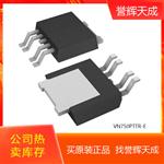
The TLV197-Q1, TLV2197-Q1 and TLV4197-Q1 (TLVx197-Q1) family of devices are part of a new generation, of low-cost, 36-V, automotive-qualified, operational amplifiers. The TLVx197-Q1 family uses a method of package-level trim for offset and offset temperature drift implemented during the final steps of manufacturing after the plastic molding process. This method minimizes the influence of inherent input transistor mismatch, as well as errors induced during package molding.
Good dc precision and ac performance including rail-to-rail input/output, an optimized cost structure, and AEC-Q100 grade 1 qualification, make this family an excellent choice for low-side current-sensing and signal-conditioning applications in the automotive space.
More unique features, such as a differential input-voltage range to the supply rail, a high output current (��65 mA), a heavy capacitive load drive of up to 1 nF, and a high slew rate (20 V/��s), make these devices a robust, high-performance operational amplifier family for high-voltage automotive applications.
The TLVx197-Q1 family of op amps is available in standard packages and is specified from �C40��C to +125��C.
�������ܣ�
����������
Ӧ������

������������ɵ�������˾
��ϵ�ˣ�����
���棺0755-82534548
��ַ���㶫ʡ�����и���������Ƽ�4����5¥505
�绰��18028704788
�ֻ���18720511991/13410894495/18720511991/ 15919489657
QQ�� 

 ѯ��
ѯ��